Technical Papers
Discover solutions to unique assembly challenges through our technical papers and presentations. Our Field Application Engineers are specialized in identifying and solving problems so if you are having assembly issues, please contact us today!
What Do You Want on Your Tombstone? – Tombstoning Defects and How to Avoid Them
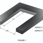
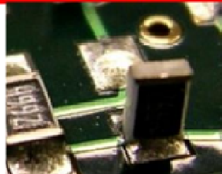
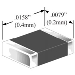
Tombstoning, draw-bridging, bill-boarding, and skewing are all common defects that are caused by movement of components out of their intended position. These defects typically occur with passive components and are a common issue for electronics manufacturers. Tombstoning, draw-bridging, bill-boarding and skewing can be caused by the circuit board design, pick and place errors, stencil design, reflow profile, and other potential sources. These potential causes of tombstoning and related defects were studied in order to create solutions for this issue. This paper summarizes the results of this work.
Fill the Void V – Mitigation of Voiding for Bottom Terminated Components
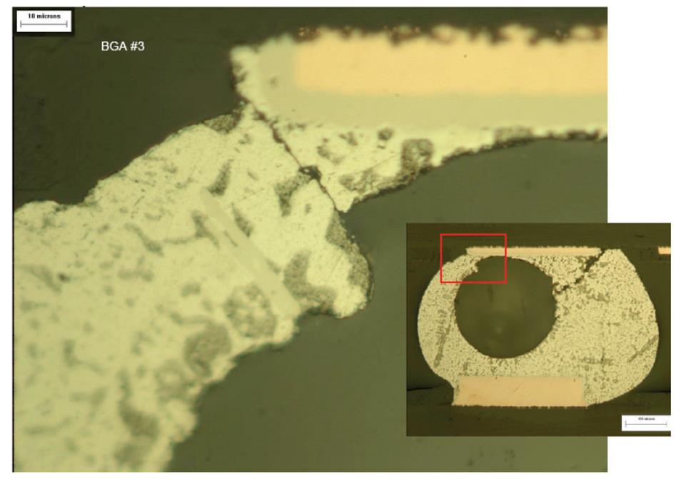
Voiding in solder joints has been studied extensively, and the effects of many variables compared and contrasted with respect to voiding performance. Solder paste flux, solder powder size, stencil design, circuit board design, via-in-pad design, surface finish, component size, reflow profile, vacuum reflow, nitrogen reflow and other parameters have been varied and voiding quantified for each. The results show some differences in voiding performance with respect to most of these variables but these variables are not independent of each other. Voiding in solder joints is a complex issue that often requires multiple approaches to reduce voiding below required limits. This paper focuses on solutions to voiding for commonly used bottom terminated components (BTCs).
The Effects of Surface Finish on Solder Paste Performance – The Sequel
This is a second study on how solderable surface finish affects solder paste performance in the surface mount process (SMT). The first study was presented at SMTA International 2018 and included print, reflow and voiding data on 6 different surface finishes run with 4 different solder pastes. This work explores some of the surface finish & solder paste combinations in more detail with an expanded set of SMT parameters. All of the test results, including data from the first study, are summarized, compared and contrasted. Discussion of the strengths and weaknesses of each combination of surface finish and solder paste are given with respect to the various SMT parameters. Recommendations are made for optimal combinations of surface finish and solder paste.
Size Matters – The Effects of Solder Powder Size on Solder Paste Performance
Solder powder size is a popular topic in the electronics industry due to the continuing trend of miniaturization of electronics. The question commonly asked is “when should we switch from Type 3 to a smaller solder powder?” Solder powder size is usually chosen based on the printing requirements for the solder paste. It is common practice to use IPC Type 4 or 5 solder powders for stencil designs that include area ratios below the recommended IPC limit of 0.66. The effects of solder powder size on printability of solder paste have been well documented.
HOW DOES SURFACE FINISH AFFECT SOLDER PASTE PERFORMANCE?
The surface finishes commonly used on printed circuit boards (PCBs) have an effect on solder paste performance in the surface mount process. Some surface finishes are non-planar like hot air solder level (HASL) which can lead to inconsistencies in solder paste printing. Other surface finishes are difficult to wet during reflow like organic solderability preservative (OSP). What is the overall effect of surface finish on solder paste performance? Which solder paste is best for each surface finish? It is the goal of this paper to answer these questions.

HOW DOES PRINTED SOLDER PASTE VOLUME AFFECT SOLDER JOINT RELIABILITY?
Printing of solder paste and stencil technology has been well studied and many papers have been presented on the topic. Very few studies have looked at how solder paste volume affects solder joint reliability. It is the aim of this work to correlate printed solder paste volume to solder joint reliability.

FILL THE VOID
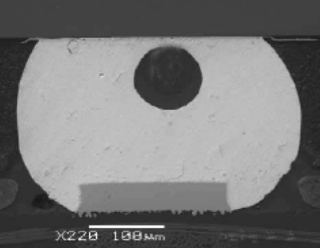
Voids in solder joints are a concern for many electronics manufacturers. They create weakness in the solder joints which can lead to mechanical failure. Voids can slow or limit heat transfer away from the component which can lead to thermal failure. Voids can also interfere with electrical signal flow creating problems with the function of the circuit board. Minimization of voiding is beneficial for the life and function of the circuit assembly.
Fill the Void II: An Investigation into Methods of Reducing Voiding
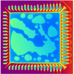
Voids in solder joints plague many electronics manufacturers. Do you have voids in your life? We have good news for you, there are many excellent ways to “Fill the Void.” This paper is a continuation of previous work on voiding in which the following variables were studied: water-soluble lead-free solder pastes, a variety of stencil designs, and reflow profiles. Quad Flat No-Lead (QFN) component thermal pads were used as the test vehicle. The voiding results were summarized and recommendations were made for reduction of voiding.
Fill the Void III
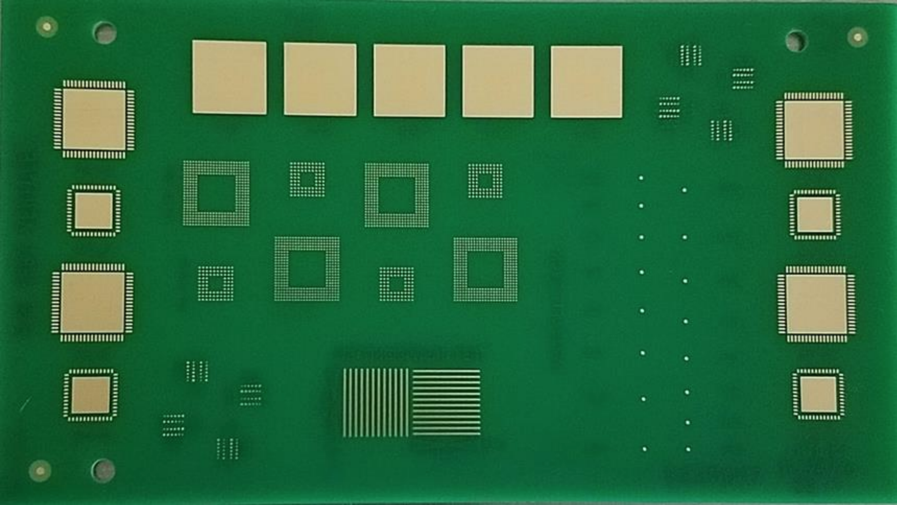
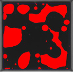
This study is part three in a series of papers on voiding in solder joints and methods for mitigation of voids. In this study several new variables were tested and compared to previous data on voiding. A new circuit board design was used which is different than the circuit board used in previous studies. The new circuit board design includes two sizes of QFNs (Quad Flat No Lead), BGA’s (Ball Grid Array), and LGA (Land Grid Array) components which are susceptible to voiding.
Fill the Void IV
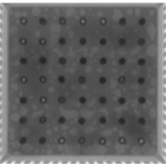
Voids are a plague to our electronics and must be eliminated! Over the last few years we have studied voiding in solder joints and published three technical papers on methods to “Fill the Void.” This paper is part four of this series. The focus of this work is to mitigate voids for via in pad circuit board designs.
An Investigation into the Durability of Stencil Coating Technologies
It is well documented that Nano coatings on SMT stencils offer many benefits to those assembling PWBs. With reduced standard deviation and improved transfer efficiency nano coatings can provide, there is also a cost. As PWB assemblers work to justify the return on investment, one key question continues to arise. What is the durability or life of these coatings and what can be done in the print process to maximize the life of the coatings? This paper addresses durability of the coatings in relation to the number of print cycles and underside wipe cycles applied as well as materials used on the underside wipe process. Different parameters will be applied and data will be collected. The results of this study will be summarized to help those using or considering the use of these nano coatings to improve their print process and suggestions will be given to maximize the life of the coatings.
Improve SMT Assembly Yields Using Root Cause Analysis in Stencil Design
Reduction of first pass defects in the SMT assembly process minimizes cost, assembly time and improves reliability. These three areas, cost, delivery and reliability determine manufacturing yields and are key in maintaining a successful and profitable assembly process. It is commonly accepted that the solder paste printing process causes the highest percentage of yield challenges in the SMT assembly process. As form factor continues to get smaller, the challenge to obtain 100% yield becomes more difficult. This paper will identify defects affecting SMT yields in the printing process and discuss their Root Cause. Outer layer copper weight and surface treatment will also be addressed as to their effect on printability. Experiments using leadless and emerging components will be studied and root cause analysis will be presented on various common SMT defects.
Step Stencil Technologies and Their Effect on the SMT Printing Process
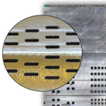
It is a common fact that the print process is one of the most critical elements in SMT production and many of today’s assemblies include both miniature components such as 0201’s, Micro-BGA’s, LGA’s and QFN’s as well as large components such as large connectors on the same assembly. Printing the proper volume of paste on these assemblies is not always possible by adjusting the apertures on single level stencils. As a result, manufacturers are finding that “Step Stencils” allow them to apply the correct amount of paste to different components on the same assembly with excellent first pass yields.
What’s coming down the tracks for Printing and Stencils
This presentation discusses trends of current and future printing technologies including new foil materials, mesh materials, new stencil lasers, nanocoatings and more.
Printing Practices for 01005 Components
01005 components are a challenge due to their size. They are popular for use in high density circuit boards including cell phones, bluetooth, wearable technologies and more. This paper explores the printing challenges and solutions when working with these small components.

Water Soluble Solder Paste, Wet Behind the Ears or Wave of the Future?
With the prevailing trend towards no-clean formulations, water soluble solder paste technology has fallen behind no-clean technology, especially for use with lead-free solder alloys. This paper details the research and development of a new water soluble lead-free solder paste that improves on the performance characteristics of existing technologies.
An Investigation into the Use of Nano-Coated Stencils to Improve Solder Paste Printing with Small Stencil Aperture Area Ratios
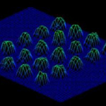
This paper presents data on small area ratio printing for component designs including 01005 Imperial (0402 metric) and smaller 03015 metric and 0201 metric chip components and 0.3 mm and 0.4 mm pitch micro BGAs. The aperture area ratios studied range from 1.06 down to 0.30. The effects of nano-coatings are studied and compared to uncoated laser cut, fine grain steel stencils.

Formulation of a New Liquid Flux for High Temperature Soldering
Through-hole soldering is alive and well in the electronics industry, despite its predicted demise at the hands of surface mount technology. Through-hole soldering is largely used for connectors, switches, and other components that require a high solder joint strength. High reliability circuit assemblies will likely use through-hole technology for many years to come.
Dispelling the Black Magic of Solder Paste
This paper presents a process for evaluating solder pastes using a variety of methods. These methods are quick to run and are challenging, revealing the strengths and weaknesses of solder pastes. Methods detailed in this paper include: print volume, stencil life, response to pause, open time, tack force over time, wetting, solder balling, graping, voiding, accelerated aging, and others. Hard data is gathered and used in the evaluation process. Also presented in this paper are a set of methods that do not require expensive equipment or materials but still generate useful data. The goal is to help the electronics assembler choose the best solder paste for their process.
Performance Enhancing Nano Coatings: Changing the Rules of Stencil Design
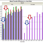
Nano-coatings are applied to solder paste stencils with the intent of improving the solder paste printing process. Do they really make a noticeable improvement? The effect of Nano-coatings on solder paste print performance was investigated. Transfer efficiencies were studied across aperture sizes ranging from 0.30 to 0.80 area ratio. Also investigated were the effects of Nano-coatings on transfer efficiencies of tin-lead, lead-free, water soluble, no-clean, and type 3, 4, and 5 solder pastes. Solder paste print performance for each Nano-coating was summarized with respect to all of these variables.
Can Nano-coatings really improve stencil performance?
This paper will present a rigorous method for evaluating the performance and economic benefits of solder paste stencil nano-coatings. Criterion such as underside cleaning, bridging, transfer efficiency across SARs, solder paste deposit geometry, post-print cleaning, and abrasion resistance of the coating, will all be considered and weighted. Performance of currently available coatings will be compared. A discussion of the economic impact on current and future SMT design will be included.
Improving SMTA Yields Leadless Components
Regardless of where one is in the world, the desire to pack “more power” into smaller devices is a common thread. Advancements in technology and miniaturization go together like peanut butter and jelly. A cellular telephone from the 1990s had considerably more computing power than what NASA had available to launch the Apollo missions in the 1960s and 1970s. The NASA computers took up rooms and rooms of space. The 1990s cellular telephone would fit into a small bag. A modern smartphone is orders of magnitude more powerful, than either, and fits into one’s pocket.
SMT Assembly Challenges and Proven Solutions for Improving Yields
Surface mount technology (SMT) assemblies are getting more complex as advancements in the areas of printed circuit board (PCB) manufacturing and component design become more main stream. Most SMT manufacturing processes have to now be capable of building “hybrid” assemblies, which contain both previous generation technology and more cutting edge technological advancements. Increasing SMT assembly yields is a must, but it is getting more and more difficult to just maintain yields, let alone increase them, as new technologies continue to be introduced.
SMT Printing Challenges
This paper discusses new developments in stencil laser and material technology and shows how these advancements, when combined, provide comparable and cost-effective alternatives to traditional electroformed stencils. The results are improved yields, cycle time reductions, and significant cost savings.
Solder Paste Stencil Printing
The introduction of the metal solder paste stencil, decades ago, to the SMT assembly process was a revolutionary change in electronics production. Wire mesh screens were the standard before then and the physics of pushing solder paste through a wire mesh severely limited aperture sizes, print volume consistency, stencil longevity, and print speed. The metal solder paste stencil dramatically improved upon all of these deficiencies.
